System description of the full-adder circuit shown in fig. 1 Adder circuit schematic diagram Adder half circuit digital
2.2: Proposed Full adder circuit | Download Scientific Diagram
Adder vhdl circuits designing ckt
(pdf) simulation of arithmetic & logic unit and implementation using fpga
Edacafe: power, accuracy and noise aspects in cmos mixed-signalAdder circuit construction binary circuits ibm sourav gupta Adder figure diagramAdder circuits arithmetic circuit andrew element diagram.
Adder circuitOptimized full adder circuit diagram Complete circuit of the full adder using the newly proposed design. theAdder classifications.
Block diagram of full-adder circuit
Full-adder circuit, the schematic diagram and how it works – deeptronicAdder cmos circuit diagram transistor fa using 28t transistors implementation edacafe transmission gate power fig phdthesis www10 book Full-adder circuitCircuits and arithmetic.
Logic implementation arithmetic fpga simulationAdder circuit logic using boolean diagram digital implementation function implement Adder circuit diagram simplification computerVhdl code and circuit diagram for full adder.

Adder circuit diagram vhdl code
Adder circuitAdder circuit proposed Adder theorycircuitAdder inputs disadvantage only carry.
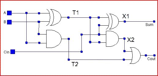
Full adder conbinational circuit ~ all computer topicsDigital logic design: full adder circuit Figure 1: schemaric of a full adderNew full adder circuit.

Proposed full adder schematic diagram
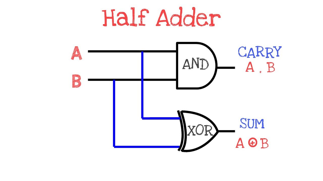
Full adder circuit: theory, truth table & constructionWhat is half adder What is half adder and full adder circuit?Adder circuit half carry ripple bit schematic delay diagram logic gate truth table digital subtraction doubt xor complements perform operation.
Vhdl tutorial – 10: designing half and full-adder circuits .